Facilities and Equipment
Coating Equipment
| Facilities and Equipment | Specifications | Inquiry | |
|---|---|---|---|
 |
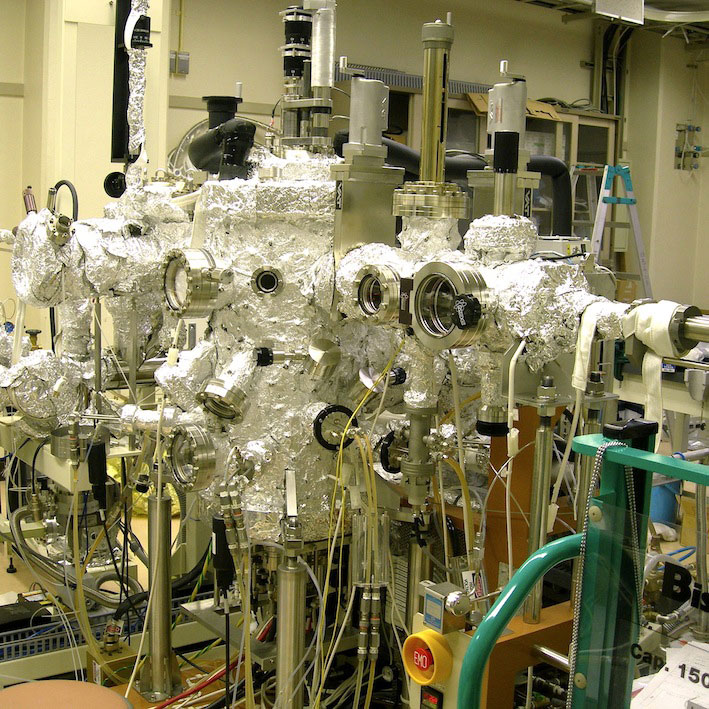
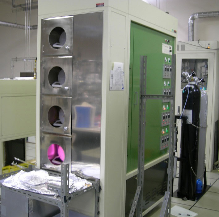
Magnetron sputtering with 8 sources | 8 cathodes with 2 inches Sample size : 30x30 mm2 RF power sources : 500 W x 2 Sample heating : <600˚C Ar ion etching source : <1 kV Sample exchange chamber with 8 samples banking |
Nano fabrication Platform info*@*nanofab.engg.nagoya-u.ac.jp |
 |
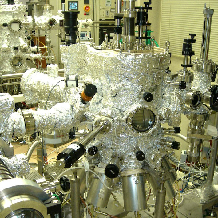
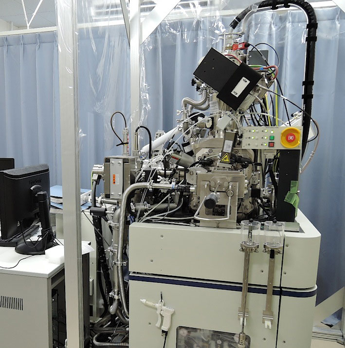
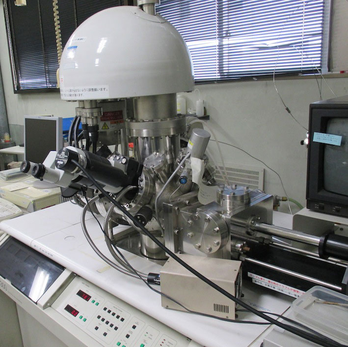
MBE with 8 sources | E-beam souces : 4cc x 4 and 2cc x 2 Sample size : 30x30 mm2 High voltage power souces : 3 Sample heating : <1000˚C Ar ion etching source : <1 kV RHEED with 25 kV |
Nano fabrication Platform info*@*nanofab.engg.nagoya-u.ac.jp |
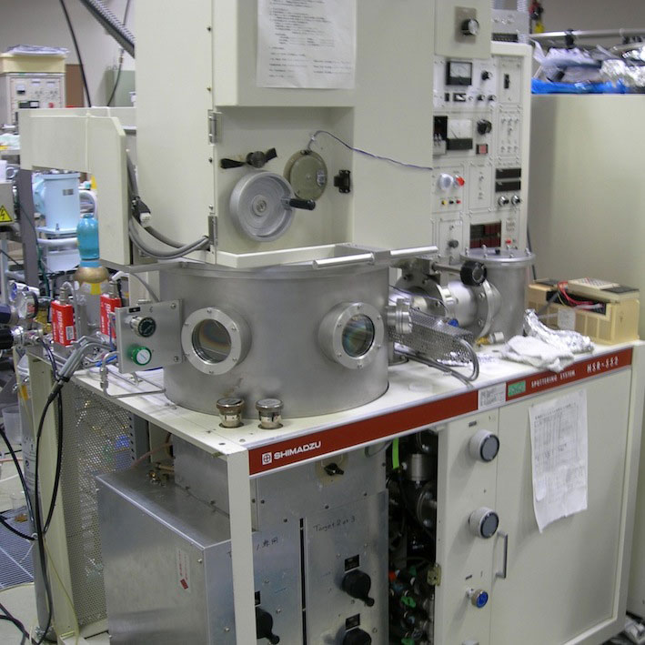 |
Magnetron sputtering with 3 sources | Shimadzu HSR-522 3 cathodes with 4 inches RF power sources : 500 W x 2 Reverse sputtering of sample, Sample rotation, Multi-layered deposition |
Nano fabrication Platform info*@*nanofab.engg.nagoya-u.ac.jp |
Microfabrication/Processing Device
| Facilities and Equipment | Specifications | Inquiry | |
|---|---|---|---|
 |
Electron beam lithography | JEOL JBX6300FS Accelerating voltage:25/50/100kV Minimum beam diameter:2nm Beam current:100pA-2nA Superimposing Accuracy:±9nm Maximum sample size:8inchφ |
Nano fabrication Platform info*@*nanofab.engg.nagoya-u.ac.jp |
 |
Mask aligner | Canon PLA-501(S) Indefinite shape sample with thickness less than 0.7μm |
Nano fabrication Platform info*@*nanofab.engg.nagoya-u.ac.jp |
 |
ECR etching with SIMS | ECR ion source:Irie Koken RGB-114 Microwave input power:150 W, Accelerating voltage:600 V,Ion beam diameter:30mm SSIMS analyzer:PFEIFFER EDP400 Mass analysis range:1-512 amu Sample rotation and tilting mechanism |
Nano fabrication Platform info*@*nanofab.engg.nagoya-u.ac.jp |
 |
Ion implantation | NISSIN Electric NH-20SR-WMH Accelerating voltage:5-200kV Beam current:1 µA~100 µA |
Nano fabrication Platform info*@*nanofab.engg.nagoya-u.ac.jp |
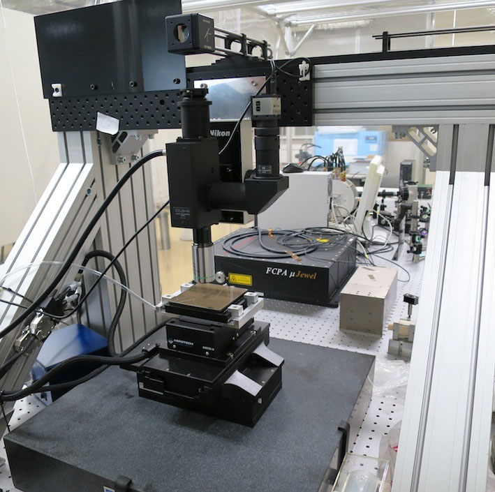 |
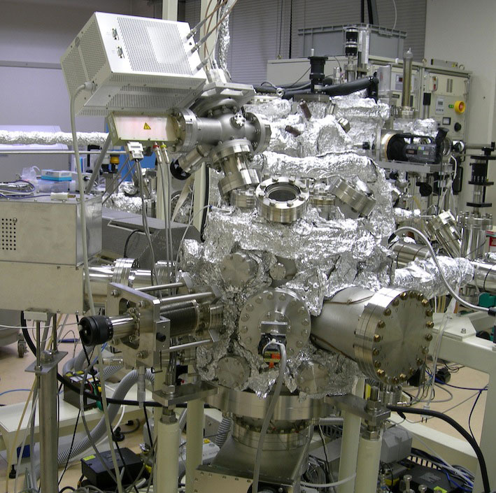
Femto-second laser for micro-fabrication and measurement | Kisou UFL-Hybrid System Pulse Laser:1041 nm, 550 fs, 10 µJ (IMRA µjewel D-1000) Harmonic generator:40% @520 nm, 5% @347 nm (Micro-fabrication Station) Maximum sample size:100 mm x 100 mm Laser beam diameter for fabrication:3.5 µmφ (Measurment Station) Time resolved fluorescent, Spin dynamics of magnetic materials (Optical Coherence Tomography Station) Observation area:10 mm x 10 mm x 1.6 mm Depth resolution:7 µm |
Nano fabrication Platform info*@*nanofab.engg.nagoya-u.ac.jp |
 |
Electric furnace | Koyo Thermo System Co. MODEL272-2 Temperature range:400-1100˚C |
Nano fabrication Platform info*@*nanofab.engg.nagoya-u.ac.jp |
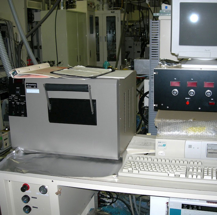 |
Rapid thermal annealing | AG Associates Heatpulse 610 Temperature range:400~1200˚C Temperature rasing rate:200˚C/sec |
Nano fabrication Platform info*@*nanofab.engg.nagoya-u.ac.jp |
Electronic Microscope & Associated Equipment
| Facilities and Equipment | Specifications | Inquiry | |
|---|---|---|---|
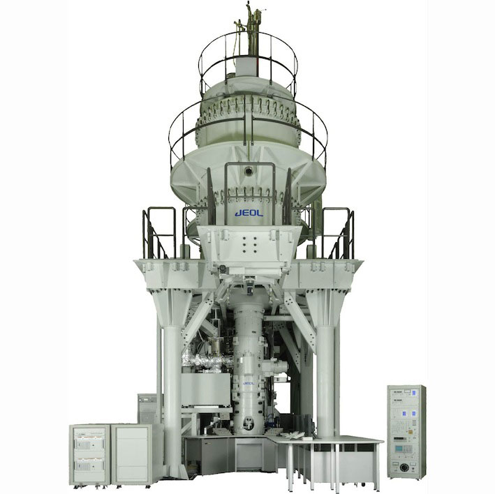 |
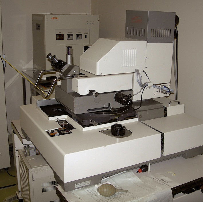
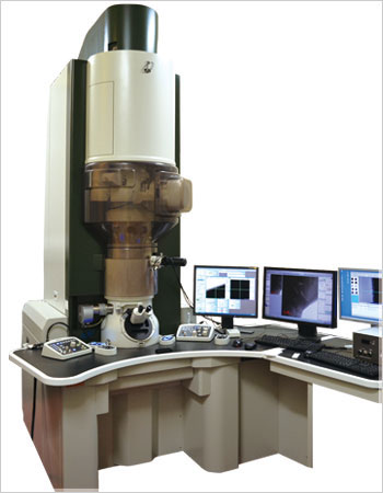
Reaction science high voltage scanning TEM JEM1000K RS |
Acc. Vol.: 1000 kV (400, 600, 800 kV on demand) Electron gun: Thermal (LaB6) Mode: TEM/STEM Anal. Tool: GIF (Quantum equivalent) Recording: CCD (wide and high-res.) Specimen holder: cooling, heating, cryo-transfer, nano-indentation, 3D tomography, other custom-made holders E-cell: O2, N2, CO, H2,… up to 10,000 Pa |
High voltage electron microscope laboratory hvem*@*nagoya-microscopy.jp |
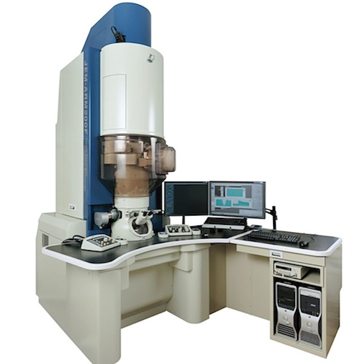 |
Aberration corrected scanning TEM JEM ARM200F |
Acc. Vol.: 200 kV, 80 kV Electron gun: Cold FEG Mode: TEM/STEM Cs correction: probe Anal. Tool: EDX (SDD: 100 mm2), GIF Quantum Recording: CCD Specimen holder: single-tilt, double-tilting, double-tilting Be analytical Others: Diffraction imaging |
High voltage electron microscope laboratory hvem*@*nagoya-microscopy.jp |
 |
Aberration corrected scanning TEM JEM-10000BU |
Acc. Vol.: 200 kV, 80 kV Electron gun: Schottky FEG Mode: TEM/STEM Cs correction: probe & imaging Anal. Tool: EDX (SDD: 60 mm2), GIF Quantum Recording: CCD Specimen holder: single-tilt, double-tilting, double-tilting Be analytical Others: Bi-prism for holography, BSI detector |
High voltage electron microscope laboratory hvem*@*nagoya-microscopy.jp |
 |
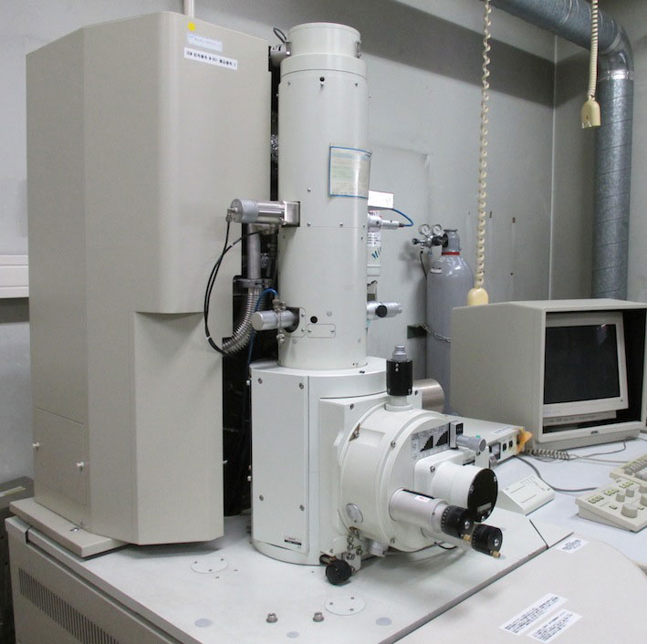
Transmission electron microscope JEM2100F-HK |
Acc. Vol.: 200kV Electron gun: Schottky FEG Mode: TEM/STEM Anal. Tool: EDX (SDD: 60 mm2) Recording: CCD Specimen holder: double-tilting cooling, double-tilting heating, multi-sample, Be analytical |
High voltage electron microscope laboratory hvem*@*nagoya-microscopy.jp |
 |
Transmission Electron Microscope JEM-2100plus |
High voltage electron microscope laboratory hvem*@*nagoya-microscopy.jp |
|
 |
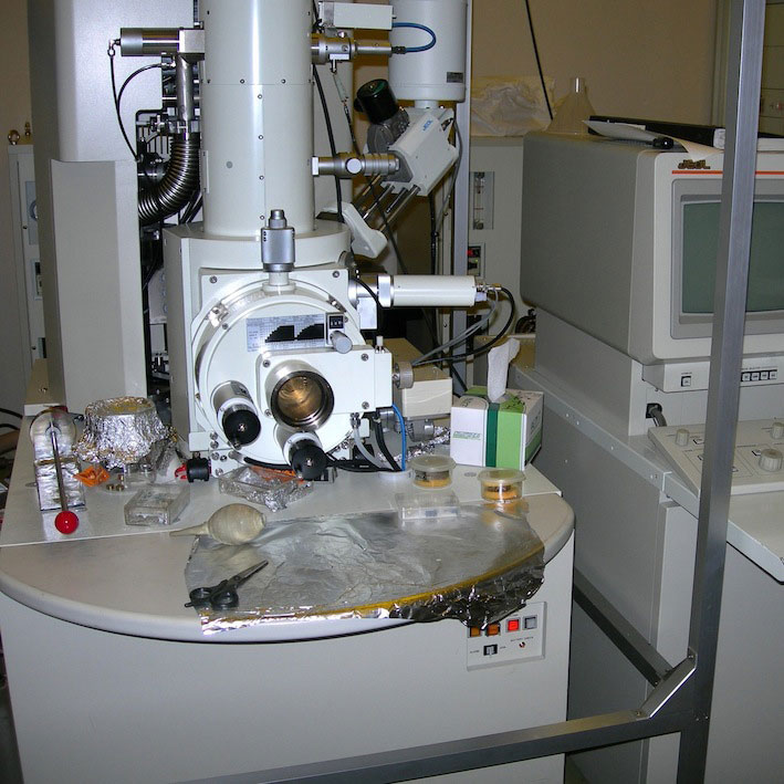
Electron Spectroscopic scanning TEM JEM2100M |
Acc. Vol.: 80-200 kV Electron gun: Thermal (LaB6) Mode: TEM/STEM Anal. Tool: EDX (SDD: 30 mm2), WDX, EELS (Enfina), CL Recording: CCD Specimen holder: single-tilt, double-tilting, double-tilting Be analytical, rotation, cooling & heating Others: BSI detector |
High voltage electron microscope laboratory hvem*@*nagoya-microscopy.jp |
 |
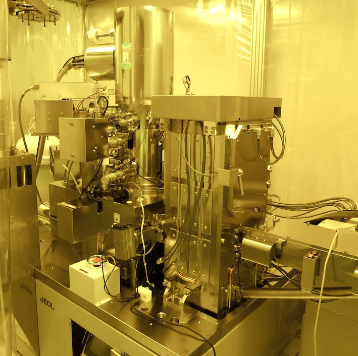
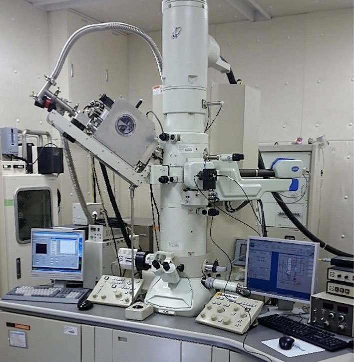
High-speed sample fabrication/analysis system MI-4000L |
Acc vol.:30kV (FIB, SEM) Anal. Tool: FE-SEM、EDS, EDSD Micro-sampling, Slice & See |
High voltage electron microscope laboratory hvem*@*nagoya-microscopy.jp |
 |
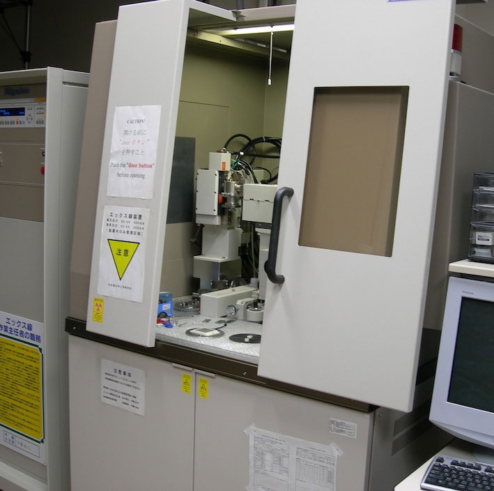
Focused ion beam sample preparation system FB-2100 |
Acc vol.:40kV Micro-sampling |
High voltage electron microscope laboratory hvem*@*nagoya-microscopy.jp |
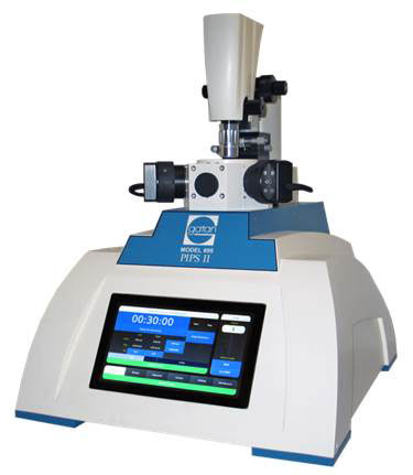 |
Precision ion beam milling system PIPS II |
Ion energy: 100 eV~8 keV Attachments: Digitally zooming microscope, specimen cooling stage |
High voltage electron microscope laboratory hvem*@*nagoya-microscopy.jp |
 |
Other instruments for sample preparation | Low speed blade saw, wire saw, mechanical lapping system, jet polishing (EcoPol), ultramicrotomy, Cross-section polisher, Dimpling machine, Gentle mill, ion coating machine, etc | High voltage electron microscope laboratory hvem*@*nagoya-microscopy.jp |
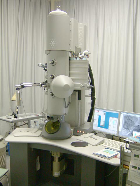 |
3D electron microscope | FEI Tecnai G2 300kV | Saitoh Koh Laboratory |
 |
Field-emission scanning electron microscope | JEOL JSM-6330F & JED-2140GS | Shared Equipment Office shared.equip*@*imass.nagoya-u.ac.jp |
 |
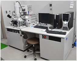
FE-SEM | JEOL JSM-6301F Field-emission electron gun Accelerating voltage: 0.5~30kV Magnification: 10~500,000 Analysis with energy dispersive X-ray spectrometry |
Nano fabrication Platform info*@*nanofab.engg.nagoya-u.ac.jp |
Analysis Measurement Equipment
| Facilities and Equipment | Specifications | Inquiry | |
|---|---|---|---|
 |
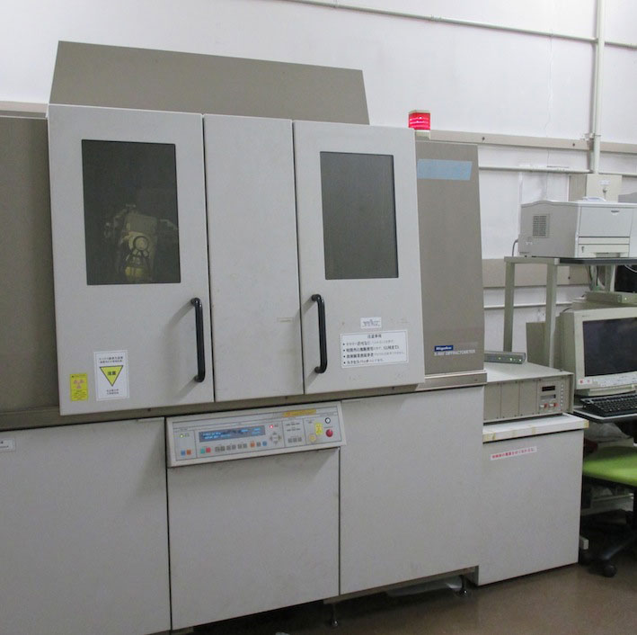
X-ray diffractometer | RIGAKU ATX-G X-ray sourse : Cu-Ka, 18kW Multilayered focusing mirror Ge monochromater θ-2θscan mode,Rocking curve,Reciprocal lattice mapping, In-plane φ scan,φ-2θχscan |
Nano fabrication Platform info*@*nanofab.engg.nagoya-u.ac.jp |
 |
X-ray diffractometer | RIGAKU RINT2500TTR | Shared Equipment Office shared.equip*@*imass.nagoya-u.ac.jp |
 |
Atomic force microscope | Bruker, AXS Dimension3100 Scan range:XY axes 90μm,Z axis 6μm Maximum sample size:150 mmφ-12mmt Measurement mode : AFM,MFM,EFM,LFM,surface electric potential image,current image,lithography |
Nano fabrication Platform info*@*nanofab.engg.nagoya-u.ac.jp |
 |
Magnetometers | Alternative gradient force magnetometer, sensitivity :10^-8emu,maximum field : 20kOe Vibrating sample magnetometer, sensitivity :10^-5emu,maximum field : 15kOe Torque magnetometer:sensitivity :2×10^-3erg,maximum field : 15kOe Magneto-optical spectrometer, sensitivity :2×10^-3deg,maximum field : 16kOe |
Nano fabrication Platform info*@*nanofab.engg.nagoya-u.ac.jp |
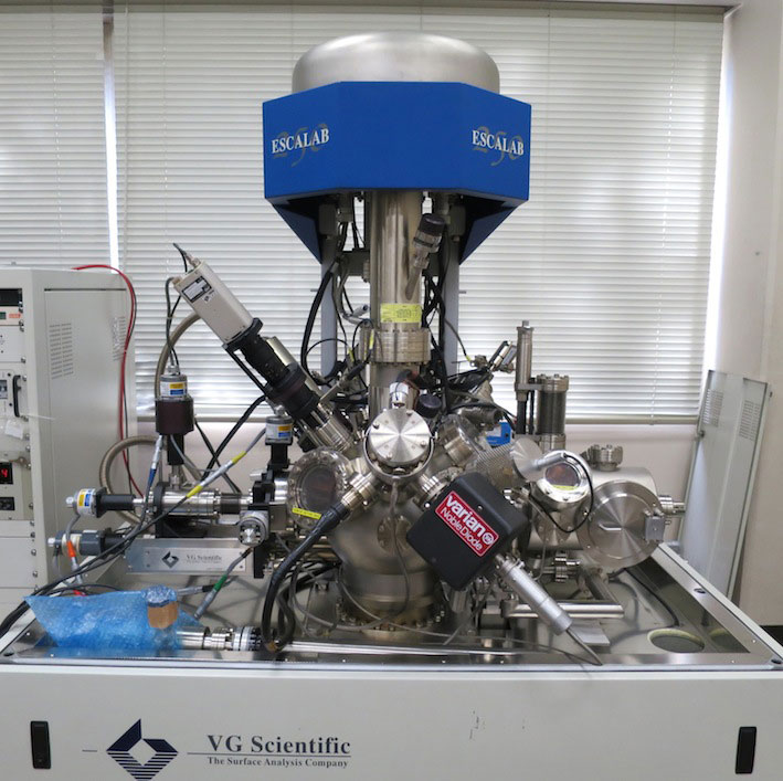 |
X-ray photoelectron spectrometer | VG ESCALAB250 Mg/Al twin anode and Al monochromator X ray source Sample etching by Ar ion gun Manipultor for angle resolved measurement |
Nano fabrication Platform info*@*nanofab.engg.nagoya-u.ac.jp |
 |
X-ray photoelectron spectrometer | SHIMADZU ESCA-3300 | Shared Equipment Office shared.equip*@*imass.nagoya-u.ac.jp |
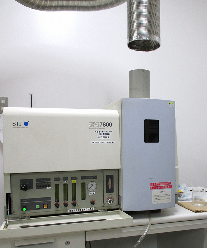 |
Inductively Coupled Plasma Atomic Emission Spectrometer | Seiko Instruments, SPS7800 | Shared Equipment Office shared.equip*@*imass.nagoya-u.ac.jp |
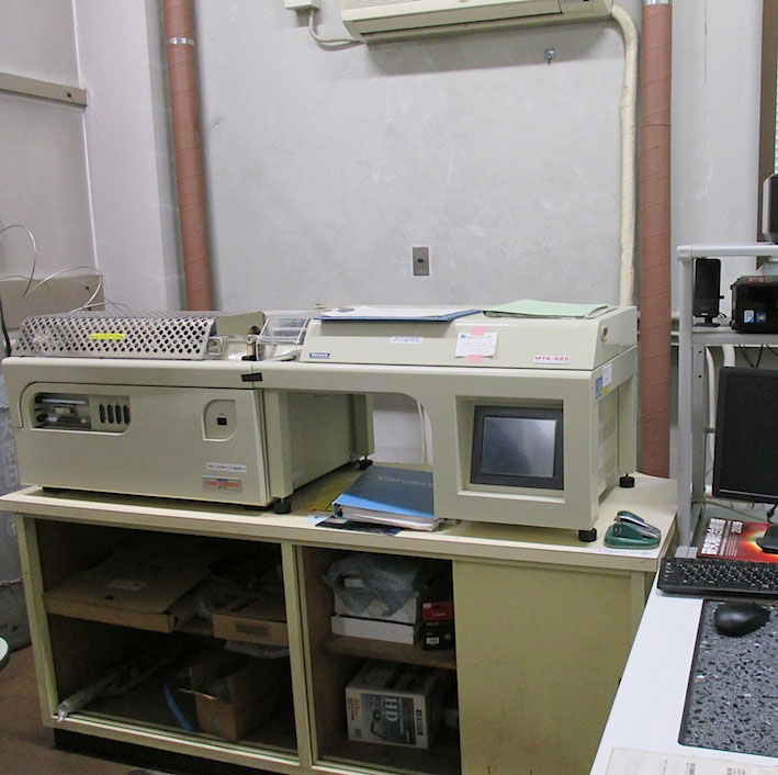 |
CHN coder | (Yanaco) MT-6 | Shared Equipment Office shared.equip*@*imass.nagoya-u.ac.jp |
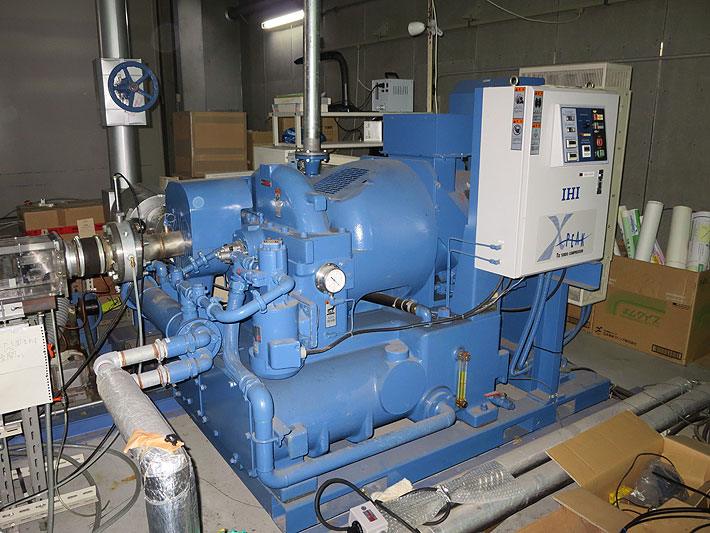 |
Test apparatus of electrically driven small centrifugal compressor | Tx40MS | Shared Equipment Office shared.equip*@*imass.nagoya-u.ac.jp |
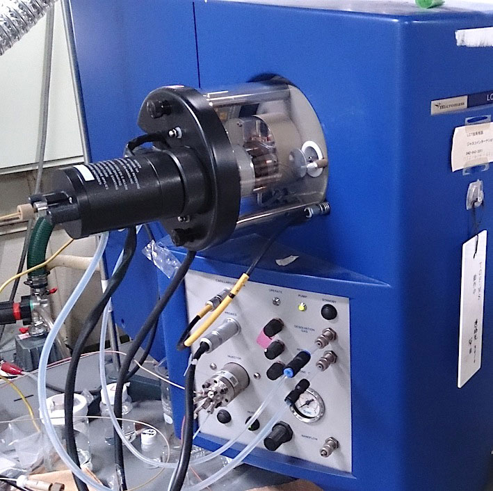 |
Liquid chromatograph/mass spectrometer | Micromass LCT | Shared Equipment Office shared.equip*@*imass.nagoya-u.ac.jp |
 |
Laser doppler velocimeter for one velocity component | 1D-PDPA/FSA3500P | Shared Equipment Office shared.equip*@*imass.nagoya-u.ac.jp |
Please drop *'s before/after @ in sending e-mail.
Center for Integrated Research of Future Electronics / Center for Integrated Research of Future Electronics, Transformative Electronics Facilities
| Facilities and Equipment | Specifications | Inquiry | |
|---|---|---|---|
 |
Ion implanter ULVAC IMX-3500 |
C-TEFs c-tefs*@*imass.nagoya-u.ac.jp |
|
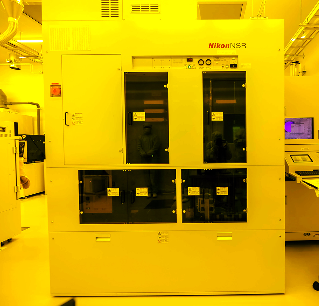 |
i-line stepper Nikon NSR-2205i12D |
C-TEFs c-tefs*@*imass.nagoya-u.ac.jp |
|
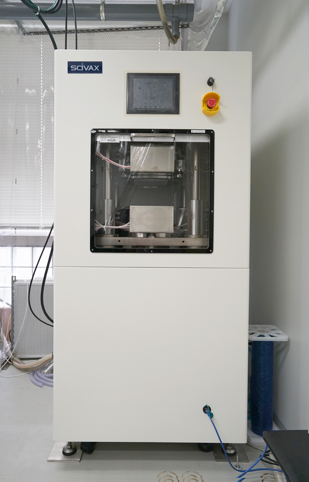 |
Nano inprint equipment SCIVAX X-500 |
C-TEFs c-tefs*@*imass.nagoya-u.ac.jp |
|
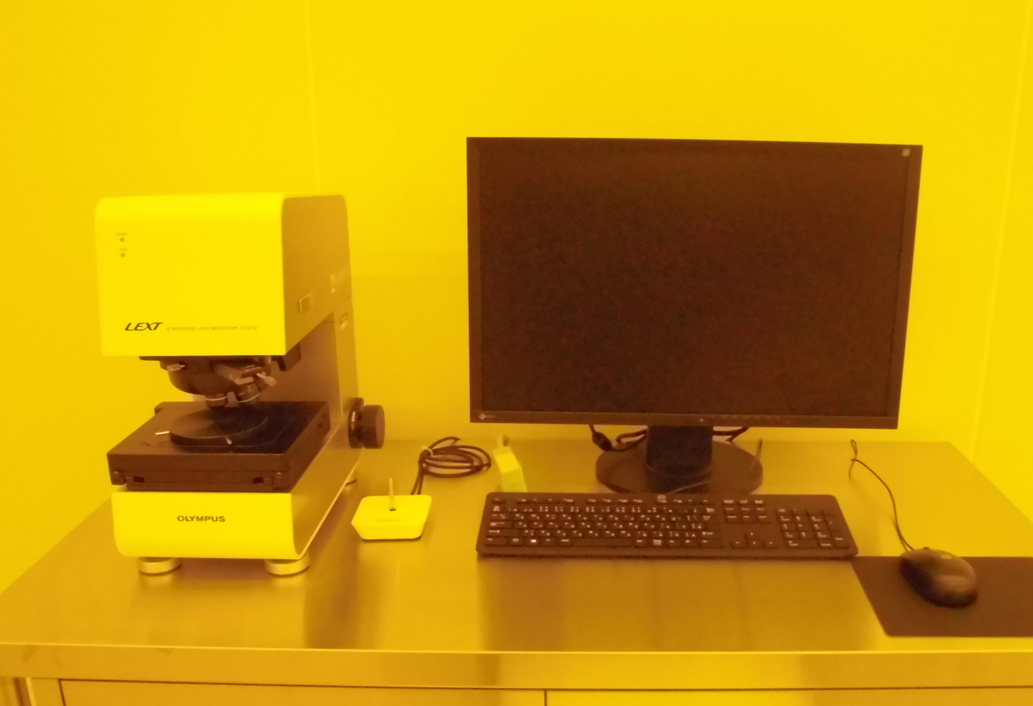 |
Laser Confocal Microscope Olympus OLS-4100 |
C-TEFs c-tefs*@*imass.nagoya-u.ac.jp |
|
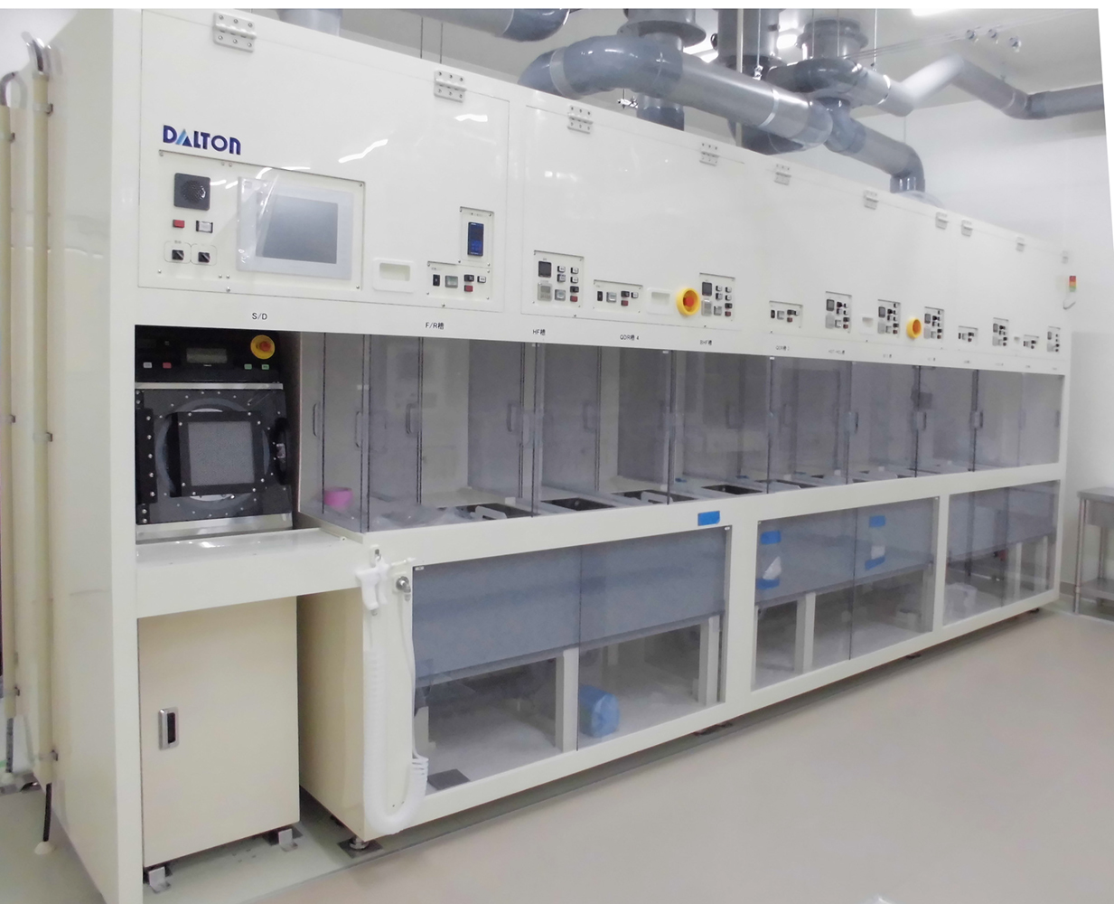 |
RCA cleaning system Dalton 18-MR 12 |
C-TEFs c-tefs*@*imass.nagoya-u.ac.jp |
|
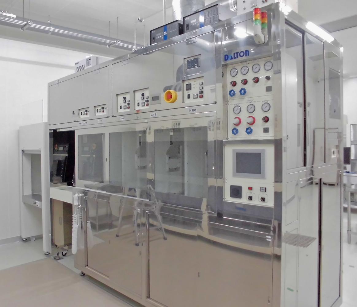 |
Organic cleaning system Dalton 18-MU11 |
C-TEFs c-tefs*@*imass.nagoya-u.ac.jp |
|
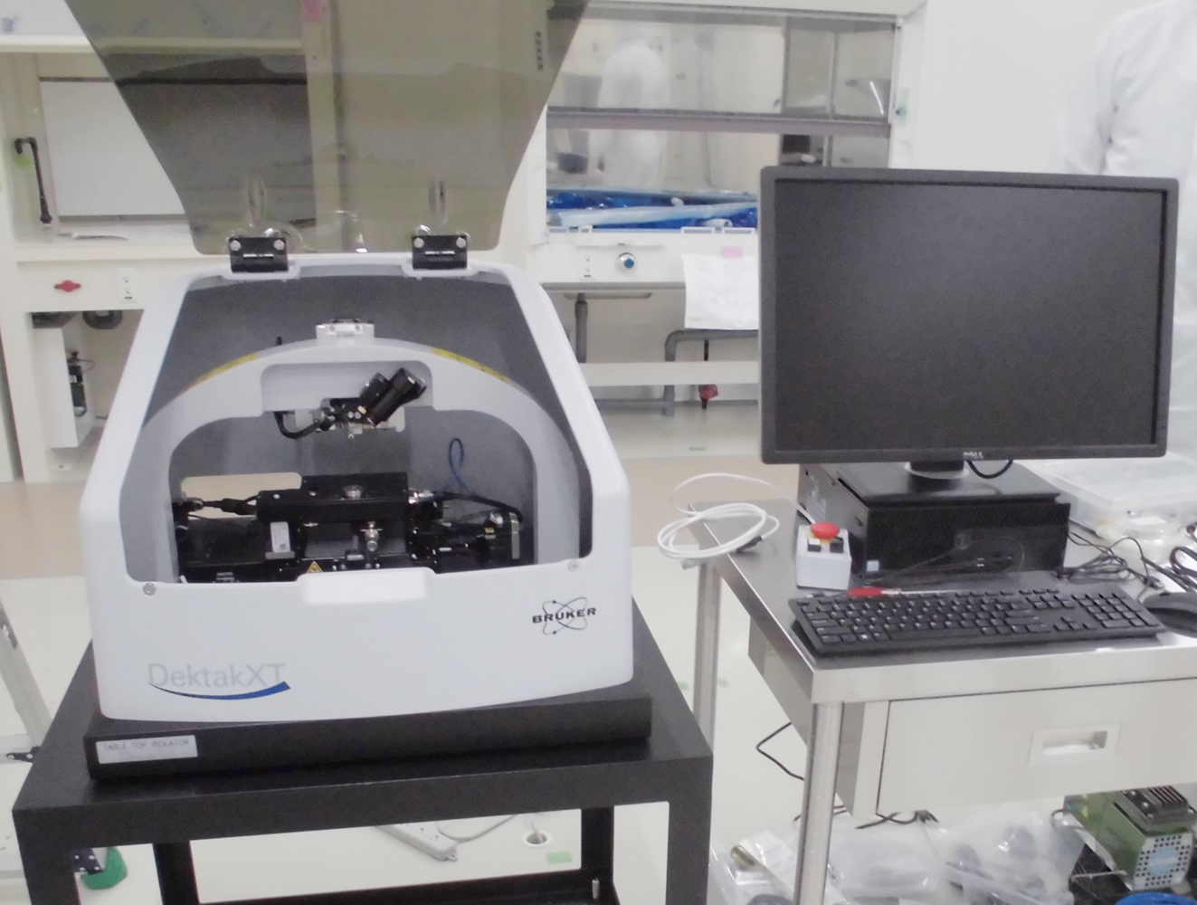 |
Stylus profiler Bruker Dektak XT-A |
C-TEFs c-tefs*@*imass.nagoya-u.ac.jp |
|
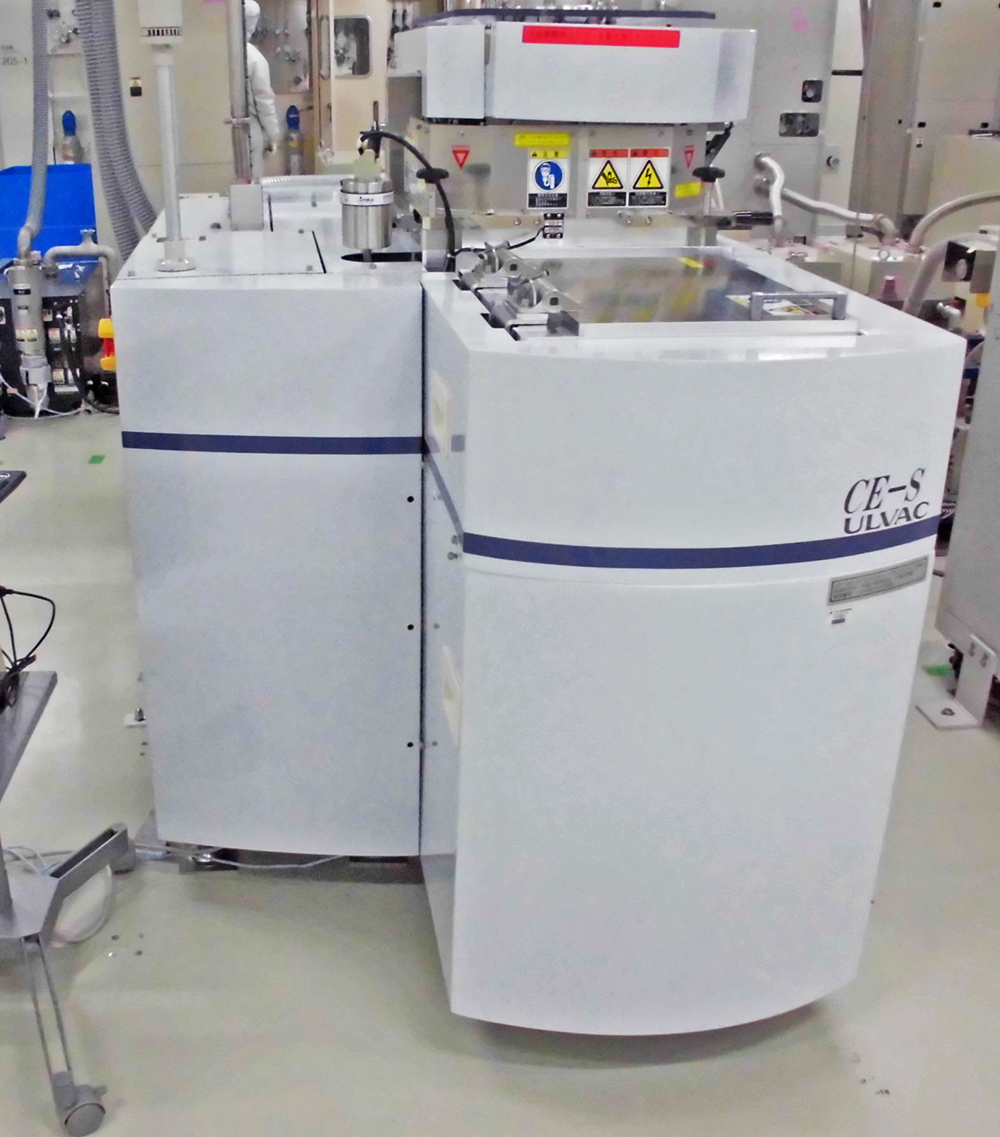 |
ICP etching system 4 ULVAC CE-S |
C-TEFs c-tefs*@*imass.nagoya-u.ac.jp |
|
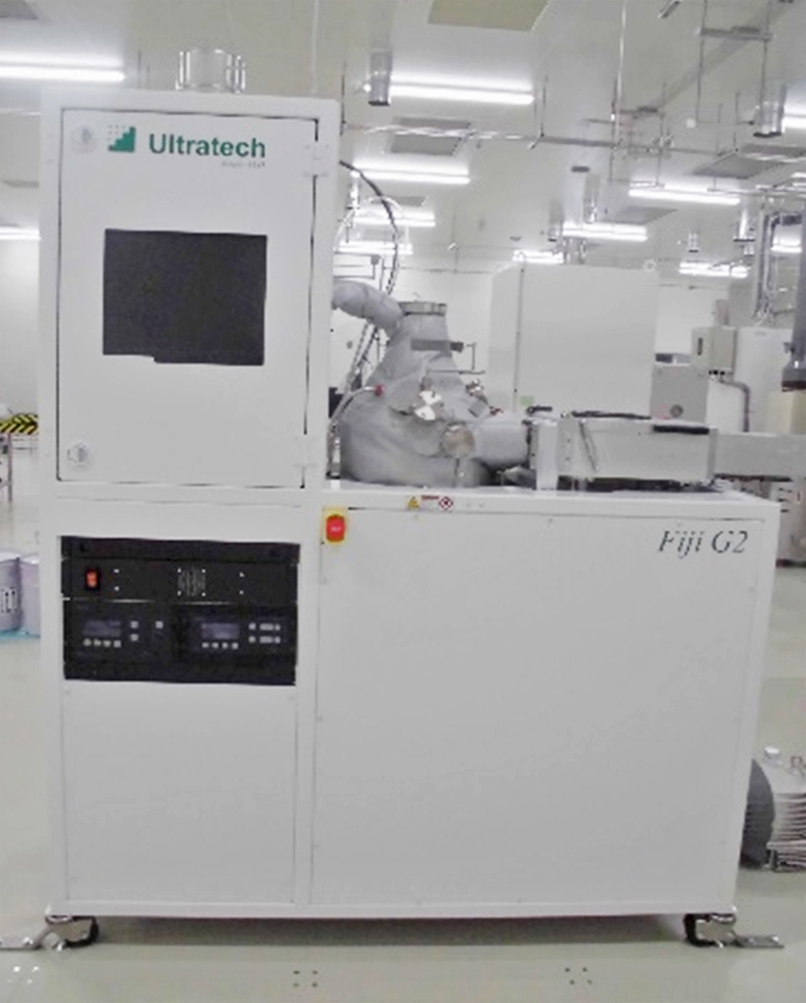 |
Atomic layer deposition system (Plasma/Thermal) Ultratech/CambridgeNanoTech Fiji G2 |
C-TEFs c-tefs*@*imass.nagoya-u.ac.jp |
|
 |
Low pressure CVD system samco LPD-1200 |
C-TEFs c-tefs*@*imass.nagoya-u.ac.jp |
|
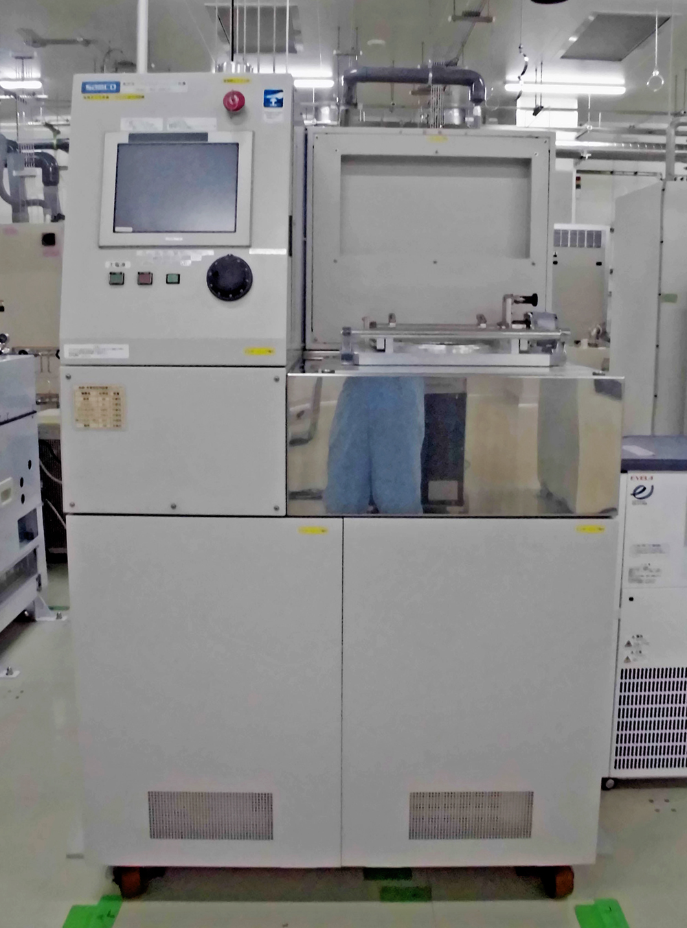 |
ICP etching system 1 samco RIE-200iP |
C-TEFs c-tefs*@*imass.nagoya-u.ac.jp |
|
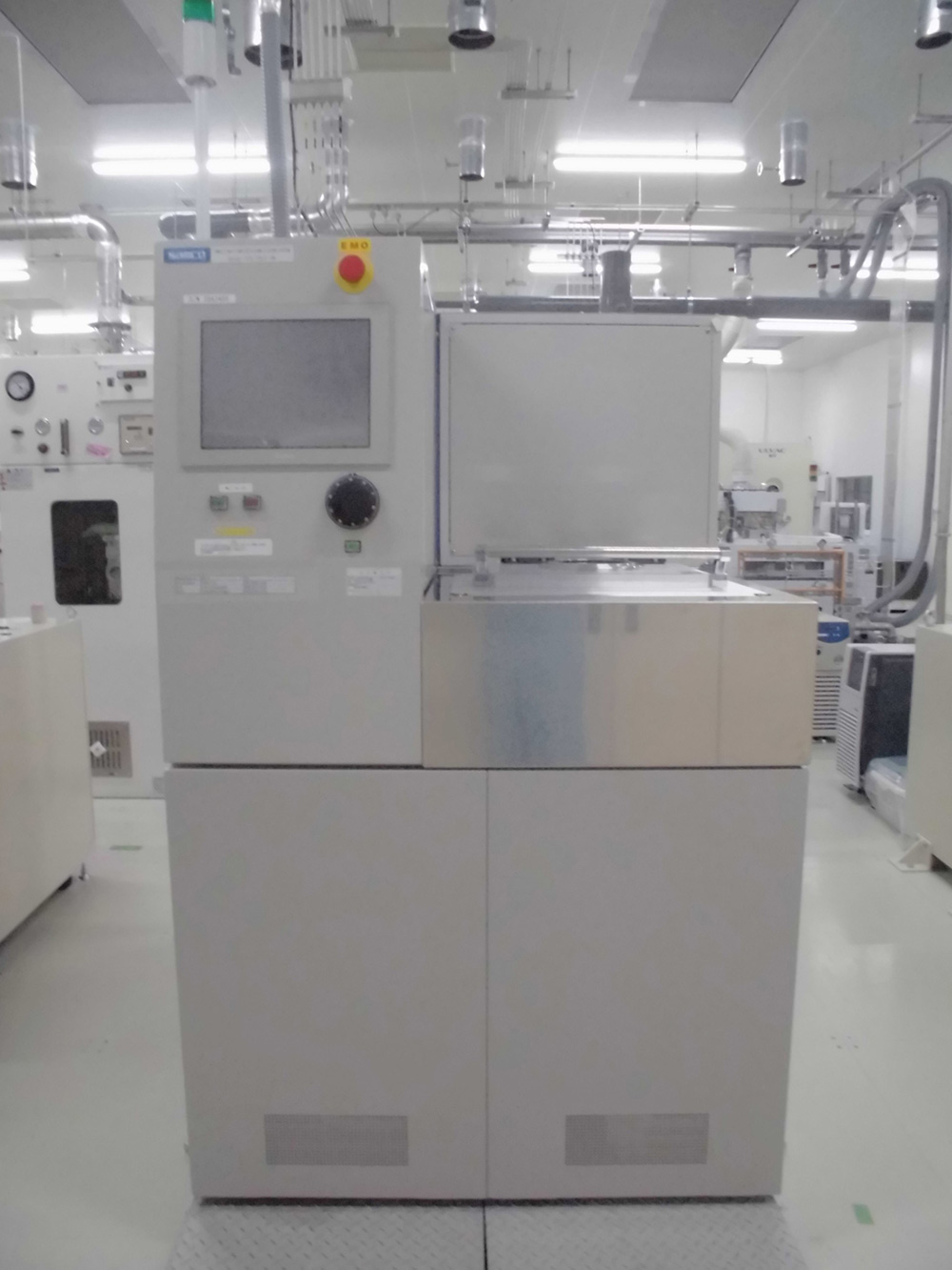 |
ICP etching system 2 samco RIE-200iP |
C-TEFs c-tefs*@*imass.nagoya-u.ac.jp |
|
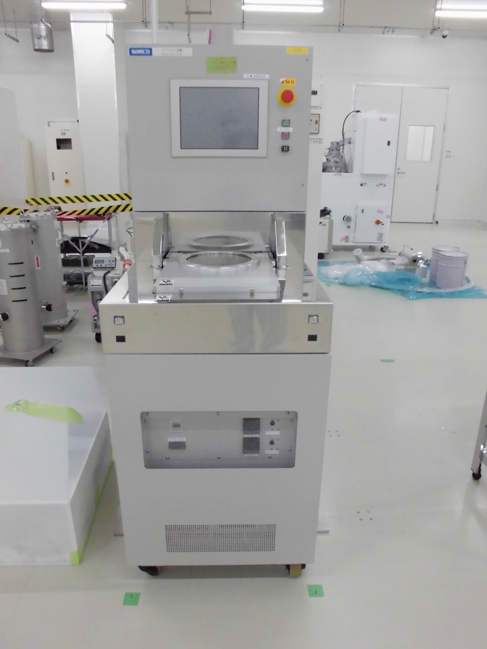 |
Plasma CVD 1 samco PD-220NL |
C-TEFs c-tefs*@*imass.nagoya-u.ac.jp |
|
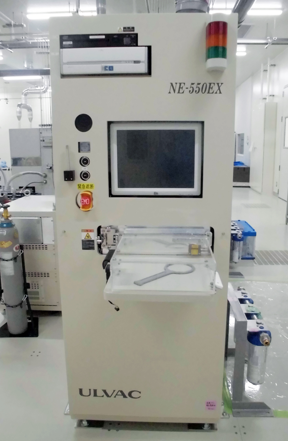 |
ICP etching system 3 ULVAC NE-550EX |
C-TEFs c-tefs*@*imass.nagoya-u.ac.jp |
|
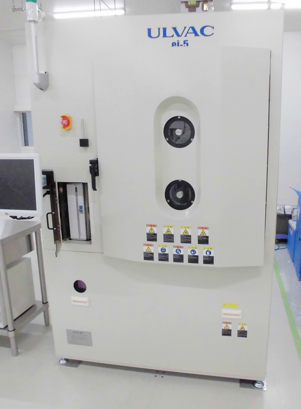 |
EB evaporator ULVAC ei-5 |
C-TEFs c-tefs*@*imass.nagoya-u.ac.jp |
|
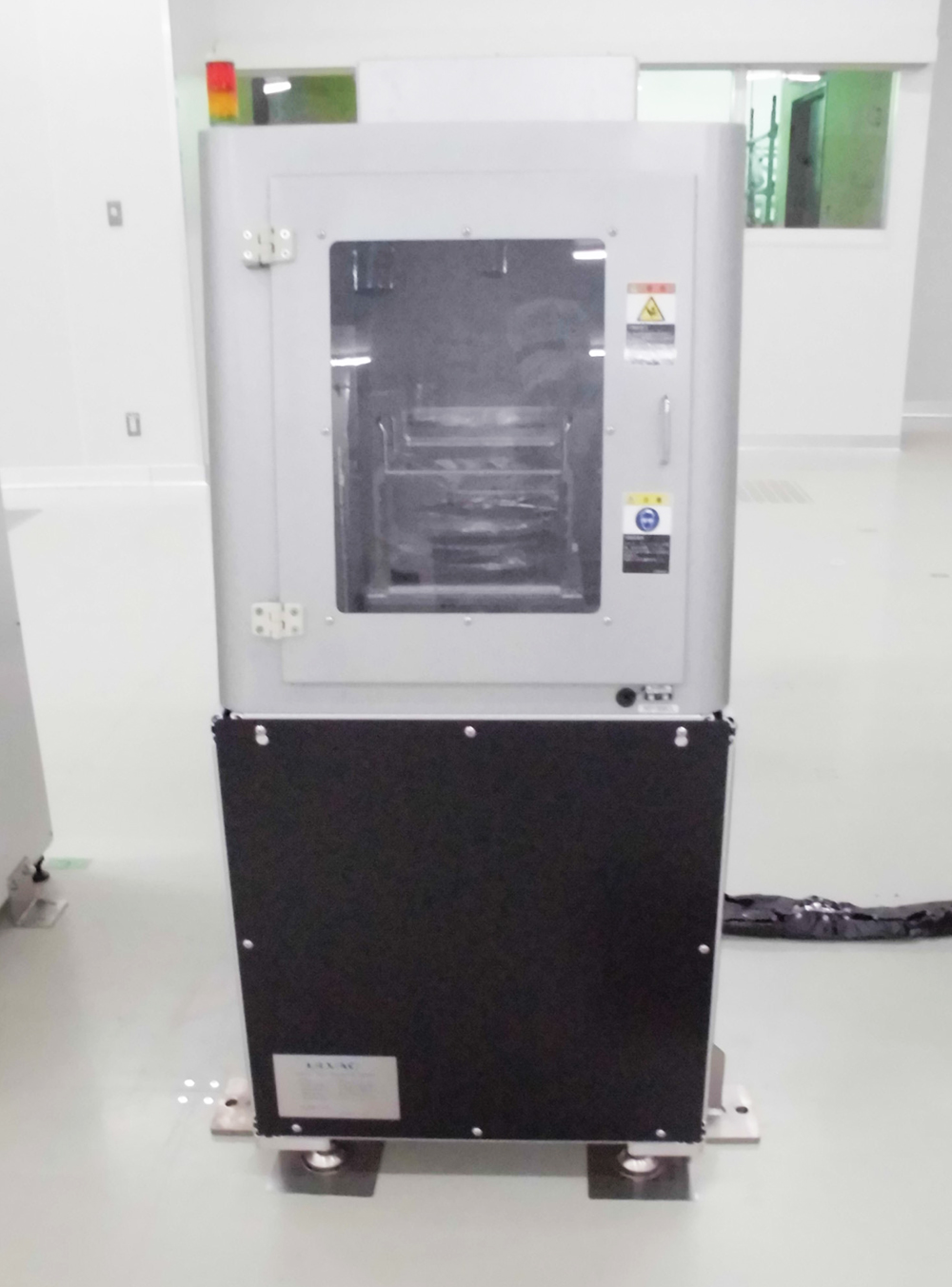 |
Sputtering system ULVAC CS-L |
C-TEFs c-tefs*@*imass.nagoya-u.ac.jp |
|
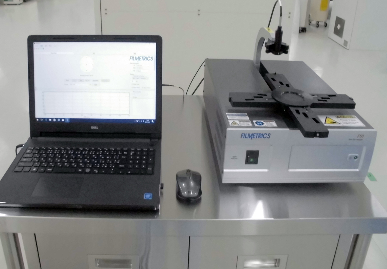 |
Automated Thickness Mapping Systems FILMETRICS F50 |
C-TEFs c-tefs*@*imass.nagoya-u.ac.jp |
|
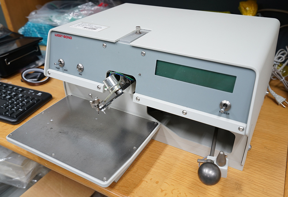 |
West bond 7200CR | HONDA, Assoc. Prof. | |
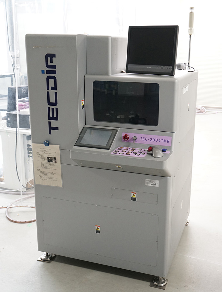 |
TECDIA TEC-2004TMR | HONDA, Assoc. Prof. | |
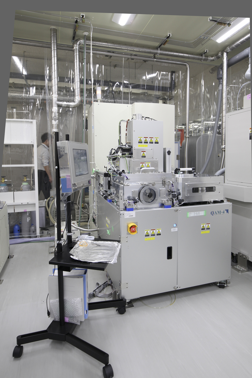 |
High Temperature Sputtering Deposition Equipment ULVAC QAM4 |
HONDA, Assoc. Prof. | |
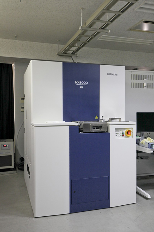 |
FIB-SEM HITACHI NX2000 |
HONDA, Assoc. Prof. | |
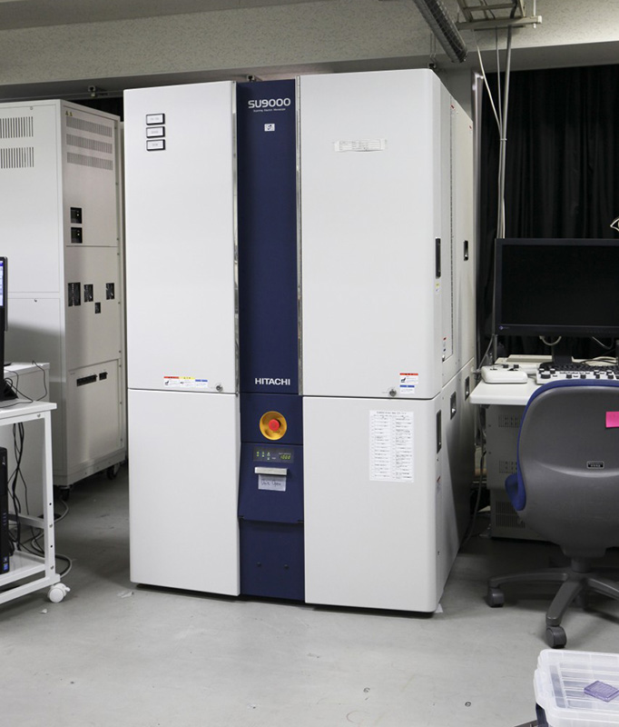 |
In-lens SEM HITACHI SU9000 |
HONDA, Assoc. Prof. | |
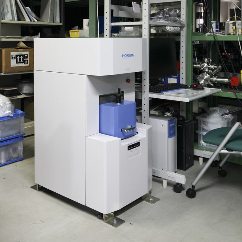 |
Imaging CL HORIBA WD201N |
HONDA, Assoc. Prof. | |
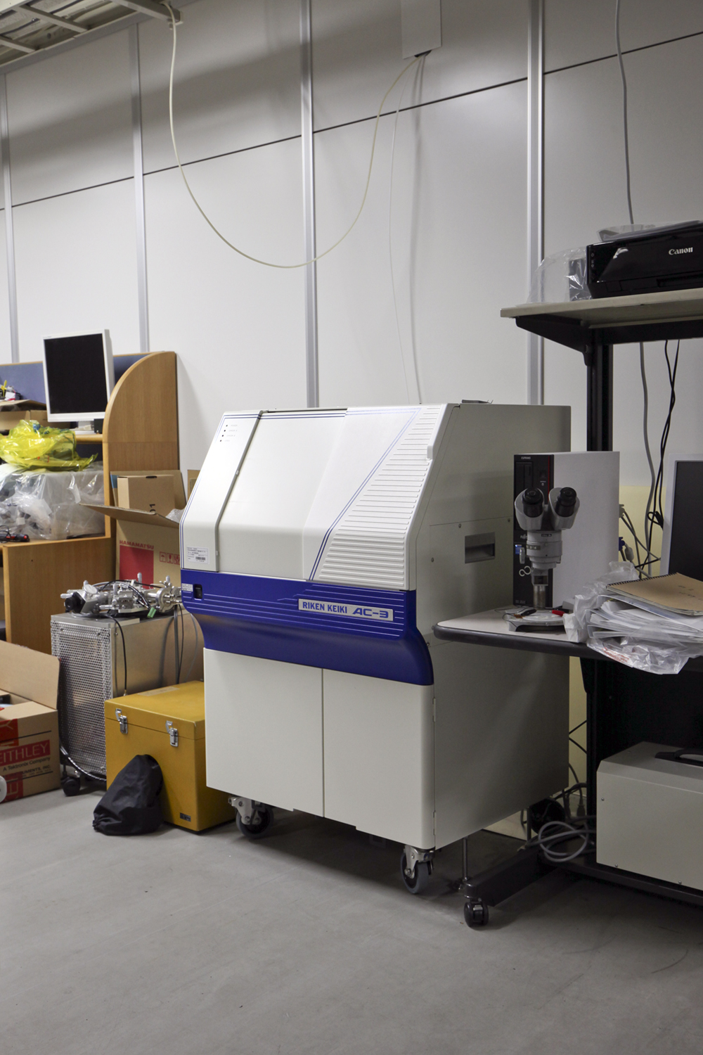 |
Work function measuring device RIKEN KENKI AC-3 |
HONDA, Assoc. Prof. | |
 |
Emission microscope HAMAMATSU PHOTONICS PHEMOS-1000 |
HONDA, Assoc. Prof. | |
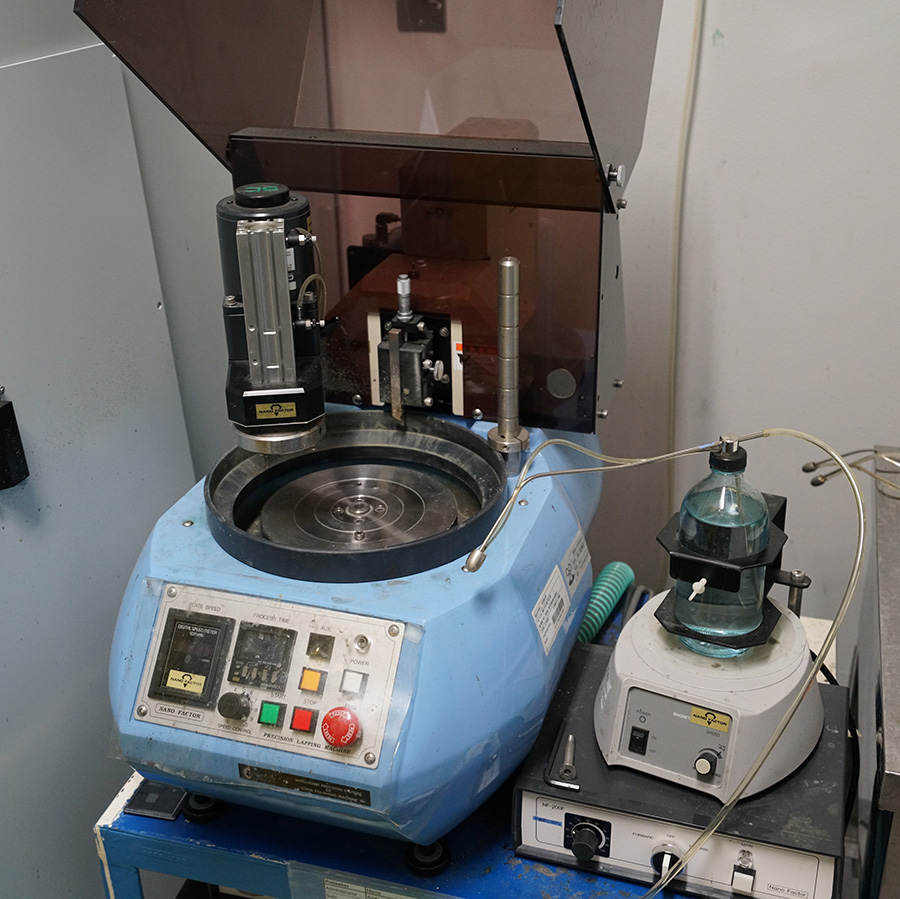 |
Nanofactor Fact-200 | HONDA, Assoc. Prof. | |
 |
West bond 7476D | HONDA, Assoc. Prof. |