This Institute has developed unique and advanced measurement technologies in the High Voltage Electron Microscope Laboratory, the Research Facility for Advanced Science and Technology, and other facilities of the Institute. The Advanced Measurement Technology Center, which was established in April 2015, aims to explore and develop novel measurement techniques, operate multiuser instruments, provide opportunities for collaborative research, and train highly skilled scientists and engineers. The Center is operated jointly by Nagoya University graduate schools and research centers with ties to this Institute, including the Graduate Schools of Engineering, Science, and Environmental Studies, and the Synchrotron Radiation Research Center, and external institutes, such as the Aichi Synchrotron Radiation Center of the Knowledge Hub Aichi and the National Institute for Fusion Science. The Center is divided into the following five sections: Electron Nanoscopy Section, Electromagnetic Wave Measurements Section, Elementary Particle Measurements Section, X-Ray Spectroscopy Section, Nanofabrication & Characterization Section.
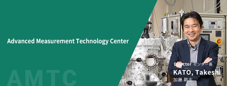
- Director of the Center : KATO, Takeshi
- Vice-director of the Center : YAGI, Shinya
Introduction video of the AMTC
Electron Nanoscopy Section
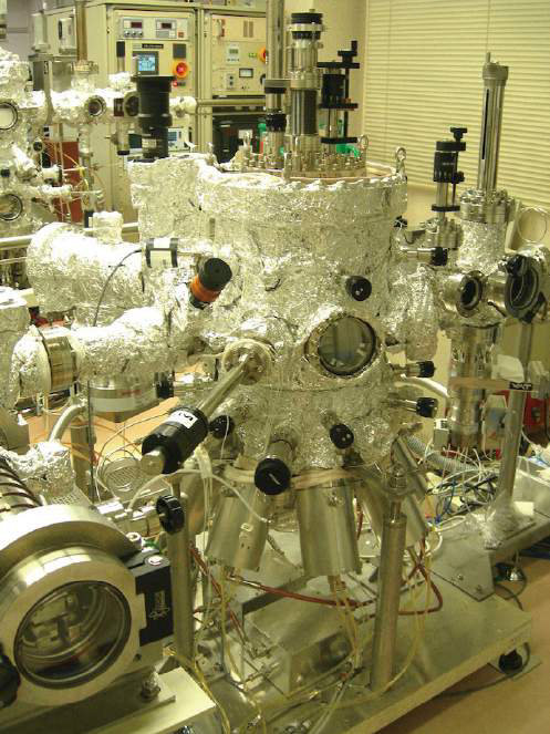
In this section, techniques for detailed structural analyses and property measurements using electron microscopes are developed. Topics include atomic-level analysis of spatial and electronic structures, precise measurements of nanoscale lattice distortions using convergent beam electron diffraction, three-dimensional structural analysis with electron beam tomography, visualization of electromagnetic fields using electron holography, and analysis of chemical reactions under different gas environments.
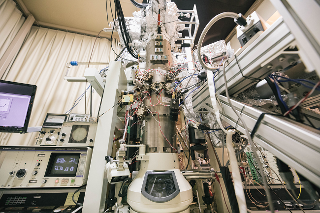
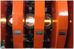
Reaction Science Ultra-High Voltage Scanning Transmission Electron Microscope JEM1000K RS
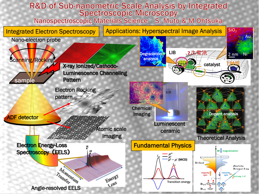
R&D of Sub-nanometric Scale Analysis
by Integrated Spectroscopic Microscopy
Nanospectroscopic Materials Science
/ S. Muto & M Ohtsuka


Spin-polarized ultrafast transmission electron microscope developed by our group


Electromagnetic Wave Measurements Section
This section is dedicated to the advancement of techniques to control energy systems, such as nuclear fusion using plasmas.
Research is focused on developing methods to measure line emissions from atoms and molecules in plasmas and reflected light from
light-emitting bodies and other materials.
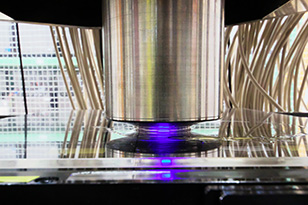
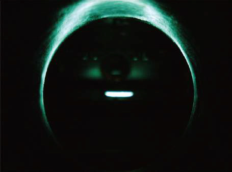
Helium plasma in the linear plasma device NAGDIS-II
and we are conducting research using plasma devices simulating the fusion conditions to control thermal particles and heat loads and
to understand material damage. In addition, utilizing surface modification by plasmas,
we are trying to fabricate novel nanostructured materials for application as, for example, photocatalysts.
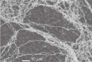
Tungsten nanowires grown
by an exposure to a helium plasma.
Elementary Particle Measurements Section
This section specializes in the development of muon radiography, which is an applied technology to obtain images inside extremely large structures (e.g., pyramid, nuclear reactor, blast furnace, volcano). This technology makes use of muons, which are elementary particles found in charged cosmic rays from outer space that hit the Earth, and other in-house conceived techniques.
Hyper Track Selector
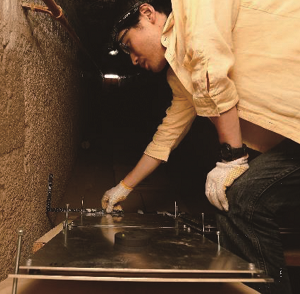
Nagoya University emulsion film setup
in the descending corridor
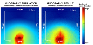
Comparison of muography simulation and results for descending corridor
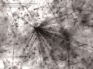
This micrograph showing the reaction that occurred when high-energy cosmic rays collided with atoms in the emulsion.
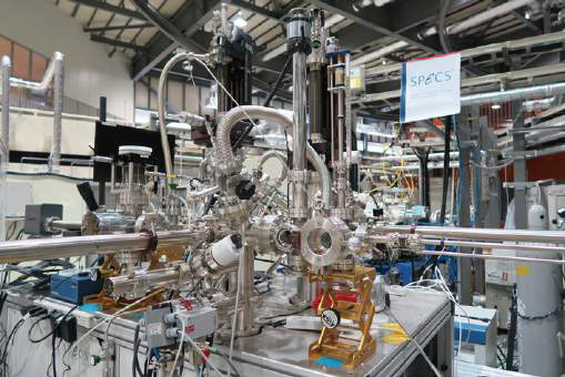
X-Ray Spectroscopy Section
In this section, innovative X-ray spectroscopy techniques using the electron storage ring and spectroscopy beamlines at the Aichi Synchrotron Radiation Center of the Knowledge Hub Aichi are pursued. In addition, applied research aimed at developing new materials and pharmaceuticals is conducted.

Nanofabrication & Characterization Section
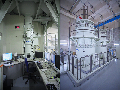
This section develops the state-of-arts techniques of thin-film deposition, nanomaterial synthesis, nanofabrication, and associated measurements and evaluations. Shared instruments and clean room at Research Facility for Advanced Science and Technology are provided for the development of advanced functional devices.
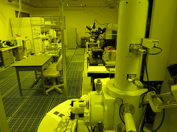
Micro-fabrication clean room