The Center for Integrated Research of Future Electronics (CIRFE), established in October 2015, engages in leading-edge electronics research-including research in the untraversed area of devices with gallium nitride, carbon nano-tube, SiC and other post-silicon materials-while also cultivating top-notch human resources to lay the foundations of the future electronics industry. CIRFE is divided into seven sections, each staffed with instructors who serve as leading specialists in their field, and equipped with outstanding research infrastructure. The Center's fully integrated joint research and education system covers everything from basic scientific education on materials, measuring, devices, and applied systems through to the completion of student educational courses. Through research on energy-saving devices, an area in which very little experimentation has been carried out anywhere in the world, CIRFE strives to foster well-trained human resources who will lead the field of manufacturing in the twenty-first century.
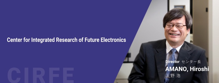
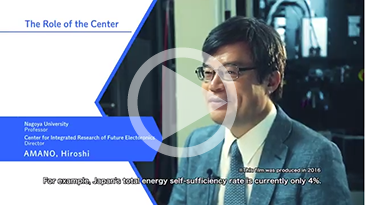
- Director of the Center : AMANO, Hiroshi
- Vice-director of the Center : UJIHARA, Toru
Introduction video of the CIRFE
Device Innovation Section
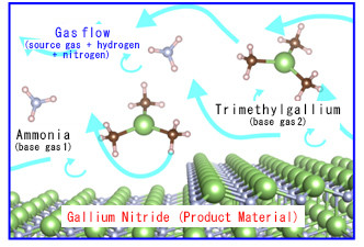
The Device Innovation Section aims to develop devices with new functions by establishing new crystal-growth methods and process development for cutting-edge electronics materials with a central focus on wide-bandgap semiconductors, such as gallium nitride and silicon carbide, and nanocarbon materials. A fully integrated research approach enables us to establish a unified process from crystal growth to device design, manufacturing, and assessment.
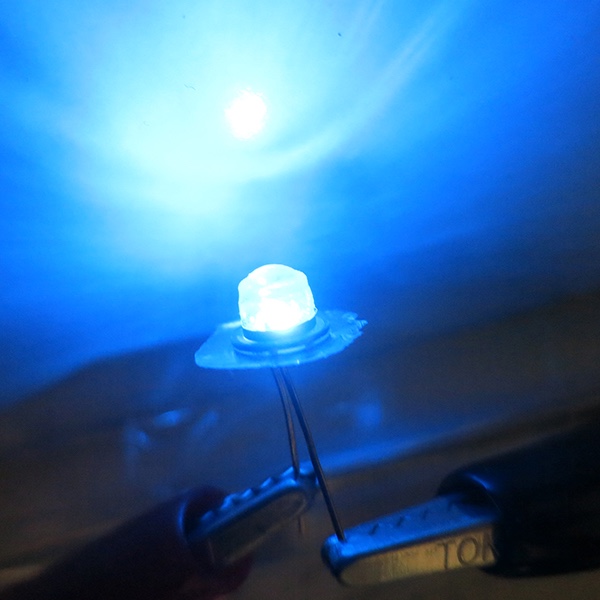
Prototype of Blue LED


Multiphysics Simulation Section
The Multiphysics Simulation Section is engaged in research with the aim of realizing multiphysical-system-based predictable crystal-growth simulations that integrate first-principles calculation with macroscopic fluid dynamics via thermodynamic analysis. Additionally,this section is pursuing proposals for new gallium-nitride-based power devices.
Crystal growth process clarified by the multi-physics simulation.


Materials Nano-Characterization Section
The Materials Nano-Characterization Section develops nanoscale operand analysis techniques for semiconductor devices under operating conditions using electron microscopy and electron holography.
These efforts are part of research centered on themes such as interface electronic properties involving direct measurement of device operations and electric-field response measurements for semiconductor interface electronic structures.
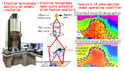
Direct electrostatic potential mapping in nano-scaled FET
under operation mode using electron holography


System Applications Section
For the purpose of realizing high-efficiency, small, and lightweight power converters and motors used in hybrid vehicles, electric vehicles, power infrastructures, and next-generation airclafts, we carry out applied research on power electronics technology by integrating fields related to power semiconductors, controlling technology, and magnetic applications. We also conduct researches for RF applications focusing on the advantages of gallium nitride (GaN) devices.

(equipped with in-wheel motors, can be fully charged by capacitor charging in 4 min compared with 5 h using conventional batteries)
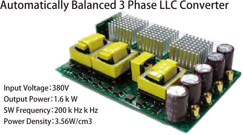
GaN power semiconductor


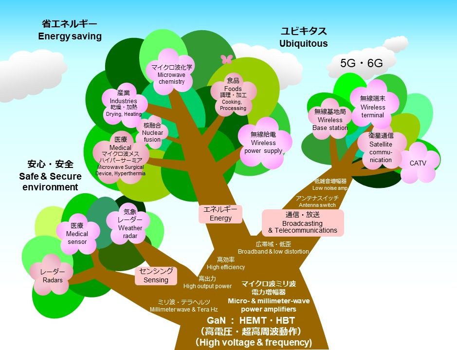
Micro- and millimeter-wave applications tree of GaN


International Research Section
In the area of devices utilizing cutting-edge electronics materials, this section focuses on the integration of such devices into various systems and pursues applied research with an eye toward real-life applications throughout society. The International Research Section engages in research and development activities together with visiting professors invited from overseas. Additionally, the Section is cultivating an international research network as part of efforts to form a central venue for nitride semiconductor research.
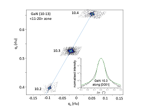
Reciprocal space map using high-resolution X-ray diffraction to estimate the basal plane stacking fault density
on (10-13) GaN crystals for green LEDs
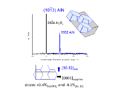
Orientation of single phase (10-13) AlN on sapphire produced by directional sputtering
and high-temperature annealing.
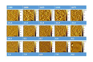
Atomic force microscope images of (10-10) AlN films prepared by metal-organic vapour phase epitaxy with three different nucleation times and annealed at different temperatures.
Numbers indicate roughness in nanometer.


Industry-Academia Collaborative Research Section
This section aims to boost the efficiency of collaborative industry‒academia research and development activities, and also serves as a mediator to help realize actual applications of CIRFE achievements and results in society.
Research strategy section
This section is established to promote implementation of gallium nitride technologies to our society. It organizes and promotes industry-academia collaborations as well as joint research projects. This section also provides a function of secretariat of GaN research strategy office of Nagoya University.