Industry–Academia Collaborative Chair
- AIST-NU GaN Advanced Device Open Innovation Laboratory
- NIMS-NU GaN Evaluation Basic Research Laboratory - Amano-Koide Collaborative Research Lab -
- Toyota Advanced Power Electronics Industry-Academia Collaborative Chair
- DENSO Automotive Power Electronics Industry-Academia Collaborative Chair
- TOYODA-GOSEI GaN Leading Innovative R&D Industry-Academia Collaborative Chair
- AsahiKASEI Innovative Devices Industry-Academia Collaborative Chair
- TOYOTA CENTRAL R&D LABS GaN Power Device Industry-Academia Collaborative Chair
- MITSUBISHI CHEMICAL GaN Substrate Devices Industry-Academia Collaborative Chair
- Rohm Multi-Scale Power System Simulation Industry-Academia Collaborative Chair
- DENSO Nano-carbon Research & Innovation Industry-Academia Collaborative Chair
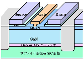
AlGaN/GaN HEMT
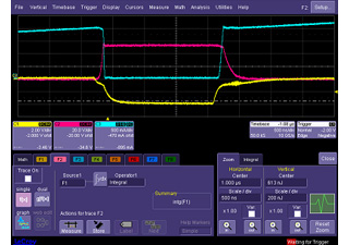
Switching characteristics
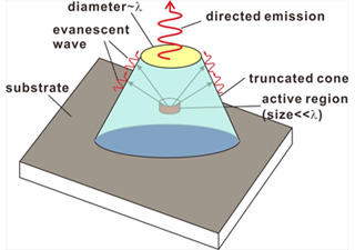
Schematic of a novel directional LED based on evanescent wave coupling
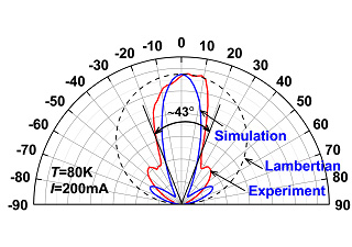
Emission pattern


1. Processing techniques that will enable the controllability of defects, impurities and damages with high accuracy
2. Device design technology for low-loss and high-switching devices
3. System applications using new gallium nitride power devices with high-performance
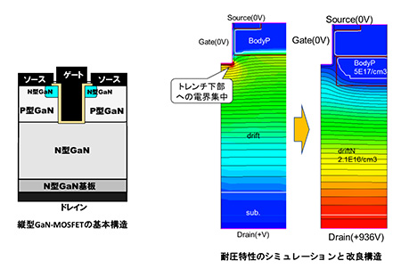
Design of vertical GaN-MOSFET structure


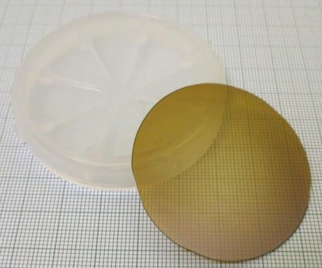
2-inch, single-crystal AlN substrate


- ①epitaxial growth with precise control of impurities and point defects
- ②gate insulators and MOS interfaces
- ③process technologies, such as low-damage etching and ion implantation
- ④device design for very low loss
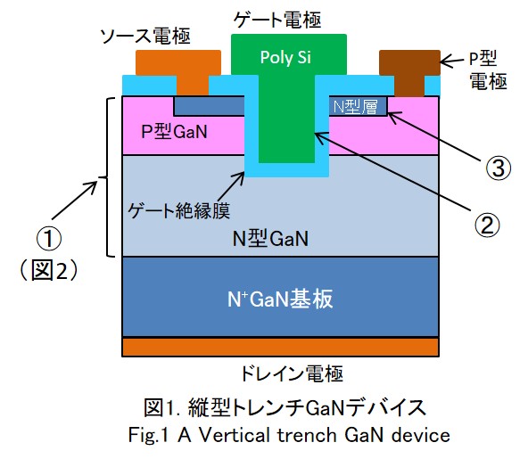
Fig.1 A Vertical trench GaN device
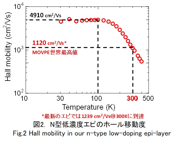
Fig.2 Hall mobility in our n-type low-doping epi-layer


- ・Investigation of the correlation between substrate quality (e.g., crystal defects, impurities)
and device characteristics, as well as elucidation of the mechanism underlying the correlation - ・Clarification of the quality and characteristics required for GaN substrates for new devices
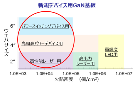
GaN substrate for new devices